


 IIT Bhubaneswar
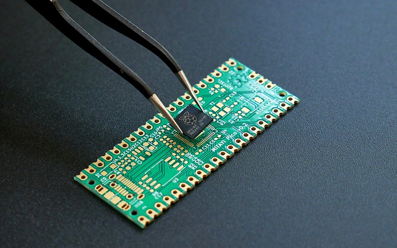
Centre approves setting up of 'NaMo semiconductor Laboratory' at IIT Bhubaneswar, check all details
Union Minister of Electronics and Information Technology, Ashwini Vaishnaw, has recently approved the setting up of the ‘NaMo Semiconductor Laboratory’ at IIT Bhubaneswar.
The project will be funded under the MPLAD Scheme.
The estimated cost of the project is Rs. 4.95 crore.
The NaMo Semiconductor Lab will contribute to Bharat’s deep talent pool by equipping the youth with industry-ready skills.
The lab will position IIT Bhubaneswar as a hub for semiconductor research and skilling.
It will help in developing talent for the chip manufacturing and packaging units coming up across Bharat, read a government statement.
The new lab will further boost the ‘Make in India’ and ‘Design in India’ initiatives.
It will act as a catalyst for the fast-growing semiconductor ecosystem of Bharat.
Bharat is home to 20% of global chip design talent. Students of 295 universities across the country are using the latest EDA tools provided by the industry.
Twenty-eight student-designed chips from 20 institutes have been taped out at SCL Mohali.
Why IIT Bhubaneswar?
Odisha has recently received approval for two semiconductor projects under the India Semiconductor Mission.
One of these is an integrated facility for Silicon Carbide (SiC)-based compound semiconductors.
The second is an advanced 3D glass packaging facility.
IIT Bhubaneswar already hosts the Silicon Carbide Research and Innovation Centre (SiCRIC).
The new lab will add to the institute’s existing cleanroom facilities. It will provide R&D facilities to support the semiconductor industry in India.
The proposed lab will have essential equipment and software required for semiconductor training, design, and fabrication.
The estimated cost is INR 4.6 crore for equipment and INR 35 lakh for software.
Support Our Journalism
We cannot do without you.. your contribution supports unbiased journalism
IBNS is not driven by any ism- not wokeism, not racism, not skewed secularism, not hyper right-wing or left liberal ideals, nor by any hardline religious beliefs or hyper nationalism. We want to serve you good old objective news, as they are. We do not judge or preach. We let people decide for themselves. We only try to present factual and well-sourced news.
Support objective journalism for a small contribution.


